CPM Seminar
Chemically synthesized CdSe quantum nanowires:
Correlations between structural, optical, and electronic properties
Tobias Kipp
Department of Chemistry
Universität Hamburg
Individual CdSe quantum nanowires (QNWs) with diameters below about 15 nm and
lengths up to several micrometers synthesized by the so-called
solution-liquid-solid method are investigated by confocal time-, energy-,
and space-resolved photoluminescence (PL) spectroscopy, transmission electron
microscopy (TEM), atomic force microscopy (AFM), and electrostatic force
microscopy (EFM).
 By correlating room-temperature PL measurements with TEM studies on the same
individual QNWs we established a detailed relationship between structural and
optical properties [1], which is mainly dictated by confinement
effects in radial direction. By combining confocal optical methods with
simultaneous EFM measurements, we showed that photo-generated charge carriers or
excitons diffuse in axial direction [2] and can be separated
in band-gap engineered QNW heterostructures [3]. By actively
charging isolated CdSe QNWs with a biased AFM tip, the PL emission can either
be enhanced or reversibly or irreversibly quenched [4]. Recent
low-temperature PL investigations revealed fundamentally new features of QNWs
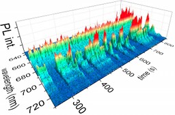
that are hidden at room temperature. In particular we observed a multitude of
sharp excitonic emission peaks arranged in two different emission bands (see
Figure at left), which exhibit a complex blinking behavior, each on a different
time scale, as well as different phonon couplings. [5]
By correlating room-temperature PL measurements with TEM studies on the same
individual QNWs we established a detailed relationship between structural and
optical properties [1], which is mainly dictated by confinement
effects in radial direction. By combining confocal optical methods with
simultaneous EFM measurements, we showed that photo-generated charge carriers or
excitons diffuse in axial direction [2] and can be separated
in band-gap engineered QNW heterostructures [3]. By actively
charging isolated CdSe QNWs with a biased AFM tip, the PL emission can either
be enhanced or reversibly or irreversibly quenched [4]. Recent
low-temperature PL investigations revealed fundamentally new features of QNWs
that are hidden at room temperature. In particular we observed a multitude of
sharp excitonic emission peaks arranged in two different emission bands (see
Figure at left), which exhibit a complex blinking behavior, each on a different
time scale, as well as different phonon couplings. [5]
In this talk, I will summarize the main aspects of above-mentioned experiments.
I will then try to draw a comprehensive picture of the structural, optical,
and electrical properties of CdSe-based QNWs that will include effects from
different diameters, crystal lattice modifications, the dielectric surrounding,
as well as from defects, like charged donors and acceptors, or surface trap
states. Finally; I will give an example of using QNWs as active elements in
photodetector devices. [6]
[1] ACS Nano 10, 7920 (2011).
[2] Nano Lett. 11, 2672 (2011).
[3] APL 100, 022110 (2012).
[4] PRL 107, 137403 (2011).
[5] Nano Lett. 14, 6655 (2014).
[6] ACS Appl. Mater. Interfaces 7, 12184 (2015)
Thursday, November 26th 2015, 15:30
Ernest Rutherford Physics Building, R.E. Bell Conference Room (room 103)
|